The Indian government has approved a major joint venture between HCL Group and Foxconn to set up a Rs 3,706-crore semiconductor facility in Jewar, Uttar Pradesh. This is an important step towards achieving India's "Atmanirbhar Bharat" (Self-Reliant India) vision and the goals of the India Semiconductor Mission. The certified facility is going to make a substantial contribution towards domestic semiconductor production through the production of display driver chips, a key component in many electronic products.
This project is likely to create tremendous job opportunities and further strengthen the growing electronics ecosystem in the nation. The sustained interest of the government in the semiconductor industry is reflected through approval for this sixth unit under the mission, reflecting consistent momentum despite earlier setbacks faced in luring such huge investments.
India's Semiconductor Ambition Takes Shape:
India has strategically put a high priority on the growth of a strong semiconductor manufacturing ecosystem as a pillar of its economic and technological growth. This strategic emphasis stems from the imperative to decrease the country's dependence on the import of semiconductors and to build self-reliance in an industry that supports the entire digital economy. The recent approval of the HCL-Foxconn joint venture for a semiconductor manufacturing facility in Uttar Pradesh is an important milestone under the overall strategy of the India Semiconductor Mission and the "Atmanirbhar Bharat" initiative, both of which are designed to make India a prominent player in the electronics value chain of the world.
The HCL-Foxconn Joint Venture: A Detailed Look
The newly sanctioned semiconductor manufacturing unit is the outcome of a collaborative venture between Indian tech giant HCL Group and Taiwanese electronics manufacturing giant Foxconn at an investment of a whopping Rs 3,706 crore. Strategically positioned in Jewar, Uttar Pradesh, the area is witnessing high-speed industrial growth with the proximity to the proposed Noida International Airport and its being part of the Yamuna Motorway Industrial Development Authority (YEIDA) zone.
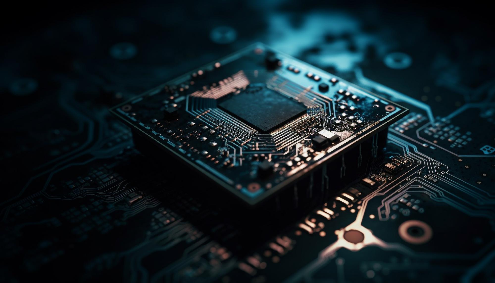
The main activity of this facility will be the manufacturing of display driver chips, which are vital parts of numerous electronic devices such as mobile phones, laptops, cars, personal computers, and many other products that feature displays. The plant has the capacity to deal with a large production volume, capable of producing 20,000 wafers in a month, which amounts to producing around 3.6 crore (36 million) chips per month. The commercial production at the plant is expected to begin in 2027. For this big-ticket investment, the government is offering approximately Rs 1,500 crore as incentives under the scheme for semiconductor manufacturing, indicating its intent to promote local chip making.
Economic and Social Impact: Job Creation and Regional Development
The setup of the HCL-Foxconn semiconductor facility in Uttar Pradesh is expected to produce a strong positive economic and social effect on the state and the nation in general. The plant is expected to generate around 2,000 direct employment opportunities in high-tech manufacturing. Apart from direct employment, the immense scale of this manufacturing plant is bound to create immense indirect employment opportunities within the supporting ecosystem of supplier industries, logistics companies, and other allied services. This establishment will give a great boost to electronic manufacturing capacities in the country, turning the focus away from import dependence and infusing strength into the domestic value chain.
Decoding the Expertise: HCL and Foxconn's Synergies
HCL Group brings to the joint venture a heritage of hardware development and a strong presence in semiconductor engineering services. The firm has developed relationships with leading semiconductor companies, such as Intel, NXP, Taiwan Semiconductor Manufacturing Company (TSMC), and Applied Materials, reflecting a profound awareness of the intricacies of chip-making. HCL's domain of expertise covers different levels of the integrated circuit (IC) fabrication process, such as lithography, deposition, implantation, etching, and testing. It is also important to note that the sanctioned factory in Jewar will manufacture compound semiconductors, reflecting HCL's entry into advanced semiconductor technology.
Conversely, Foxconn is a worldwide leader in electronics production and the world's largest electronics contract manufacturer, producing Apple's very successful iPhone, among other products. Foxconn has leading technologies in chip packaging, such as wafer-level packaging, which is of particular applicability for display driver chips. The tie-up between HCL and Foxconn is an efficacious synergy that marries the design and engineering strengths of HCL with Foxconn's huge manufacturing capabilities in a strong partnership to produce semiconductors in India. Foxconn has a whopping 40% stake in this strategic joint venture, reinforcing its seriousness to pursue this alliance